Summer Diaries: Australian National University
September 5, 2019
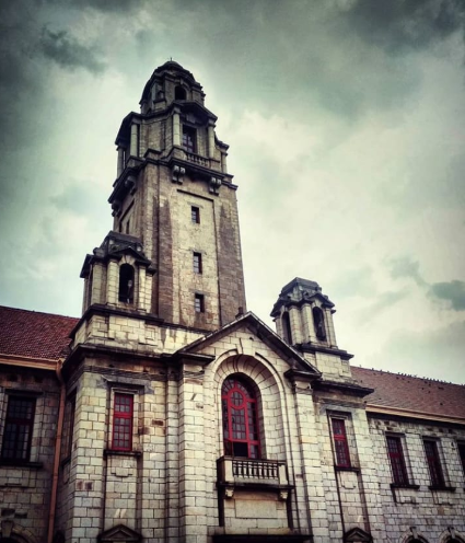
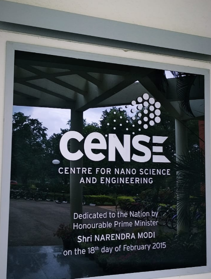
The CeNSE ( Center of Nanoscience and Engineering ) was established in 2010 at Indian Institute of Science Bangalore, to pursue interdisciplinary research across several disciplines with a focus on nanoscale systems. Current research topics include, but are not limited to nanoelectronics, MEMS/NEMS, nanomaterials and devices, photonics, nano-biotechnology, solar cells and computational nano-engineering. The centre has been built around two central facilities: National Nanofabrication Centre (NNfC) and the Micro and Nano Characterization facility (MNCF). Both are national user facilities, i.e. they are accessible to outside academic and industrial users that include scientists from other departments in IISc DRDO, ISRO and other such scientific establishments in the country.
Supporting the central facilities are the MEMS and IC Packaging lab, the Computational Nanoengineering (CoNe) laboratory, Systems Lab, and 14 other functionally distinct laboratories managed by various research groups headed by a faculty members coming from a diverse background.
I had worked on two interrelated projects on the campus. The first one was related to fabrication of perovskite quantum dots in the chemistry department, a new generation zero dimensional photoluminescent material that has immense potential to be used in the field of light emitting devices and solar cells. The second one was in the field of interface dynamics of heterojunction organic solar cells in the electronics and communications department. Fiddling with the field of alternative solar cells, I wanted to expand my breadth and learn the skills that were prerequisite in the field. Further, working in a year and a half in the campus. I came face to face with few shortcomings that are unfortunate for an undergraduate student, especially if you are an experimentalist. They are mainly centered around the availability of the material characterization and other facilities in Institute Instrumentation center and other labs all over the campus.
As explained by the multiple research intern diaries before, the most popular and effective way to land a research internship is by writing curated emails to professors, research groups and at times, even to the PhDs or postdocs working in the labs. And if you are in the second year, and have a fairly low CG like me ( < 6.5 ), this remains the only effective option, striking out the options of research programs. I was fairly pessimistic about my chances but anyways, looking at my peers doing the same, started emailing professors in India. There are a few things that one must take care while mailing which helps to increase the acceptance chances.
Try to focus on your strengths. If you are a student with a high C.G and comparatively research output, that can be a selling point.
Try to highlight the skills that you possess and can make you a useful addition to the group. This includes courses that you have took and the projects you have done under some professor or tech group on the campus.
This is the most important that the mail should be highly professor centric. One of the best time saving ways that you can follow if you are doing some research project under some professor is to make small notes of the research papers that you are anyways studying during the literature review. If the papers are relatively new, in the last 5 years or so, you can be fairly sure that the professor is still working in that field. Write an email to the professor or Ph.D. that includes your observations combined with the possibilities that can be done. Make sure that you don’t include your current work in that if you don’t want to face the wrath of the in-campus professor you are working in.
Keep emailing and mailing, and if the offers come, fair and good, if they don’t you are only in second year are in one of the premier institutions in the country where you can develop your skills or kickstart a long project that is more likely to yield you research papers than a 2 month long internship.
I started mailing after the winter vacations to professors from IISC, IITs, IISERs and a couple of other research-centric institutes like TIFR, CSIR. Initially, I was met with plain rejections, unreplied emails or professors redirecting me to their research programs. A couple of weeks before the endsems, I got lucky and got acceptance from two professors, one from CenSE, IISC Bangalore and other from CSIR-CGRI Kolkata. The former being one of my initial targets and better prospects, other than having friends from the campus in Bangalore and IISC, was my final choice. The last advice: If you have a low CG and want to get in research, increase it, and if you can’t make sure that you don’t give up, keep mailing and doing research.
Indian Institute of Science (IISc) is one of the oldest, and the most prestigious research and educational institutions in India with departments researching specific areas. The Centre for Nano Science and Engineering (CeNSE) was established in 2010 to pursue interdisciplinary research across several disciplines with a focus on nanoscale systems like MEMS/NEMS, nanomaterials and devices, photonics, nano-biotechnology, solar cells, and computational nano-engineering. The center has been built around two central facilities – The National Nanofabrication Centre (NNfC) and the Micro and Nano Characterization facility (MNCF). Both are national user facilities, i.e. they are accessible to outside academic and industrial users. Supporting the central facilities are the MEMS and IC Packaging lab, the Computational Nanoengineering (CoNe) laboratory, Systems Lab, and 14 other functionally distinct laboratories managed by various research groups.
My project was a part of a larger project that was funded by the Government of India (GOI) and focussed on fabrication of low-cost GaAs solar cells on a multifilm substrate consisting of Germanium and Silicon. The entire duration of the complete project is a few couples of years with multiple research groups collaborating on the different aspects of the project. To give you a basic idea, GaAs solar cells are highly efficient, but due to their high cost, they are only used in intergalactic space. If their cost can be reduced, this will mark an important milestone in the undergoing solar revolution, with the rural areas in our country benefiting the most.
Its a known fact that Bangalore’s weather is the best out of all the metros, and if you couple it with IISc’s lush green campus, you are in for a perfect getaway from the summer heat that has plagued me all these years. My contribution to the project could be branched out in three parts:
Analyzing the XRD patterns to determine the crystallinity of the laser annealed germanium over silicon. Crystallinity is extremely important to allow charge carrier transport and I guess this is where my material science background was specifically of help to my mentor.
Designing a LabVIEW virtual instrument. After carrying out initial experiments, we had to carry out zig-zag motion of laser beam on the specimens. For this, linear stages were procured and they needed to be programmed with the help of LabVIEW which further attaches them to the rest of the fabrication apparatus.
Literature Review: Laser annealing of semiconductors is a fairly old field since the 1970s and extensive knowledge of its existing literature had to be known if we were to explain all our results and the one which was to follow.
The work environment was pretty chill and we could come and leave anytime we wanted to as long as we could show considerable progress in our reports, submitted once a week during group meetings. IISc is a premier research institution where you can attend lectures, seminars, and conferences which are happening every day at some of the other department. Other than giving you a good idea of where the research in the world is heading to, its free lunch, and possible networking hub with like-minded people. I used to do most my work in the M.Tech lounge where the other interns also used to sit, chit-chatting with them on Bean Bags, playing a game of Counter-Strike, or strolling around the campus in on rented bicycles. Bangalore being a metro city is too crowded, but if you go in the outskirts, you can go for short night treks to the hills and the monoliths that border the city. Pondicherry as the french seaside town is just a night drive away. Apart from that, if you want to enjoy it that conventional way, you can go to beautiful bookstores, breweries, and cafes and can attend quizzes and concerts.
A research internship, especially in IISc in the second year was an eye-opening exercise for me. You get exposure to people who have been in the field for decades and get to learn the essential skills. Away from the noisy confused background of IIT, and being so close to what it actually is, it definitely does help to answer one’s question, if one wants to continue doing research or not. The biggest takeaway for me was the availability of XRD, SEM, etc. which takes a month or two to avail in Roorkee, but a day or maximum half a week in here. Talking to professors, even possible disputed Nobel Laureate and students from all over the country coupled with roaming in a city that is littered with gardens, history, and perennially beautiful weather was one of the few wholesome experiences I have had in my life!